Most semiconductors are based on ultrapure silicon because it is able to form a glass oxide on top of the wafer, which in turn, can be patterned with photolithography to enable the production of complex integrated circuits.
In the manufacture of semiconductors, photolithography is critical. This refers to the production of metal lithographic printing plates through acid etching. To break it down, lithography is the process of producing the patterns on the semiconductor crystals that will be further used as integrated circuits. The principle behind this is the simple characteristic that oil and water do not mix. Lithographic plates are usually made from grained and anodized aluminium that has been subjected silicate to form a durable water-receptive surface. Said plates consist of:
- image areas: This part is oil-receptive (oleophilic) and therefore water repellent. Basically, an area for which printing is possible.
- non-image areas: The part of the plate where printing is not possible. This is therefore made from a water-receptive (hydrophilic) and oil-repellent (oleophobic) material.
These characteristics of the lithographic plate guarantee that when the printing plate is dampened by rollers, only the non-image areas are wetted; and when it is inked with rollers, the image areas easily accept the oily lithographic ink.
In the electronics version, processing of copper printed circuit boards is involved. This is similar to the photolithographic steps of semiconductor processing.
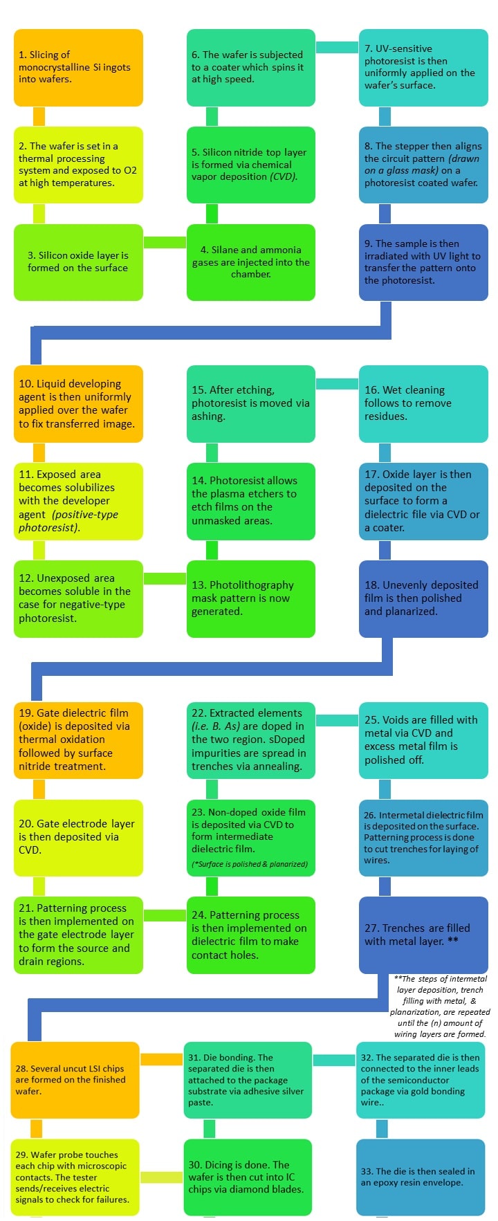
To summarize the process of manufacturing semiconductors, there are 30 simplified steps:

In the manufacture of semiconductors, specific standards are set in place; from the design phase up to the fabrication and testing. As per the American National Standards Institute (ANSI), semicnductors device standards focus on IEC published series: IEC 60747, 62047, 61290, and 61292. Normally, the application the semiconductor is intended for dictates its properties.
It is critical to have a Grade A or ISO Class 5 environment in the manufacture of semiconductors to guarantee that no contamination will null the efficiency of these electronics.
References:
- Anon. (2020). Semiconductor Manufacturing Techniques | Solid-state Device Theory | Electronics Textbook. Retrieved 13 December 2020, from https://www.allaboutcircuits.com/textbook/semiconductors/chpt-2/semiconductor-manufacturing-techniques/
- ANSI. (2020). Other Semiconductor Standards. Retrieved 13 December 2020, from https://webstore.ansi.org/industry/semiconductors/other
- Clean Room & ISO Classifications. (2020). Retrieved 13 December 2020, from https://www.americancleanrooms.com/cleanroom-classifications/
- Czochralski Process - an overview | ScienceDirect Topics. (2020). Retrieved 13 December 2020, from https://www.sciencedirect.com/topics/chemistry/czochralski-process
- Merriam-webster.(2020). Definition of LITHOGRAPHY. Retrieved 13 December 2020, from https://www.merriam-webster.com/dictionary/lithography
- ScienceDirect. (2020). Semiconductor Manufacturing - an overview. Retrieved 13 December 2020, from https://www.sciencedirect.com/topics/engineering/semiconductor-manufacturing
- ScienceDirect. (2020). Silicon Wafer - an overview. Retrieved 13 December 2020, from https://www.sciencedirect.com/topics/materials-science/silicon-wafer
- Tokyo Electron Limited. (2020). How Semiconductor is made | nanotec museum. Retrieved 13 December 2020, from https://www.tel.com/museum/exhibition/process/process8.html
Recommended Products


